
Telecom
Electronic Industry
Medical industry PCB's
Automotive industry
Telecom
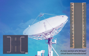
5G/4G, wireless communication, digital TV, mobile phone, fiber optic communication, communication equipment, radio frequency, Bluetooth, radio
Electronic Industry
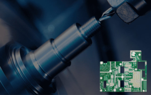
The consumer electronics industry demands high performance technology to be complex and compact at the same time.
Medical industry PCB's

The medical field requires a vast level of technology with extreme reliability and long term life cycles.
Automotive industry

The automobile industry must have circuit boards that are extremely reliable with an emphasis on safety.
Electric vehicles, automotive electronics,